Wednesday, December 31, 2008

Weekly Patent Review

Kodak filed an application US20080315272 on control of 4T pixel floating diffusion capacitance in such a way that it's low for small signals and large for large signals. The pixel schematics is shown below:


Transistor 201 opens only for large signals, increasing floating diffusion capacitance to accomodate the larger charge.

Omnivision's application US20080318358 talks about using indium doping for the photodiode pinning layer. Indium allows for a shallower implant layer with higher concentration than commonly used boron. An indium-boron combination is also applied for the patent.

Tuesday, December 30, 2008

Image Sensors on Electronic Imaging 2009 Symposium

2009 IS&T/SPIE Electronic Imaging Science and Technology Symposium will be held on January 18-22 in San Jose. The conference has a full track on image sensors and related areas. Below are just few of the most interesting papers to be presented on the Symposium:

Nanoplasmonic filters for image sensors
Author(s): Stephane Getin, Yohan Désières, Catherine Pellé, Olivier Lartigue, Ludovic Poupinet, Laurent Frey, Commissariat à l'Energie Atomique (France)

Potentially these filters can substitute today's organic ones. I wonder how far they have to go till the mass production.

An ultra fast 100 ps, 100µm 3D pixel imager
Author(s): Alex Kluge, Pierre Jarron, Jan Kaplon, Petra Riedler, Teemu S. Tiuraniemi, Fadmar Osmic, CERN (Switzerland); Giulio Dellacasa, Gianni Mazza, Angelo Rivetti, Sorin Martoiu, Angelo C. Ramusino, Massimiliano Fiorini, Istituto Nazionale di Fisica Nucleare (Italy); Elena Albarran Martin, CERN (Switzerland)

A global electronic shutter pixel using pinned diodes fabricated in standard CMOS image sensor technology
Author(s): Keita Yasutomi, Shizuoka Univ. (Japan); Toshihiro Tamura, Photron Ltd. (Japan); Masanori Furuta, Toshiba Corp. (Japan); Shinya Itoh, Shoji Kawahito, Shizuoka Univ. (Japan)

It's interesting to see Toshiba eying toward global shutter solution.

Low Gr-Gb sensitivity imbalance 3.2M CMOS-image sensor with 2.2-μm pixel
Author(s): Nagataka Tanaka, Junji Naruse, Hirofumi Yamashita, Ikuko Inoue, Makoto Monoi, Toshiba Corp. (Japan)

It's nice to see that Toshiba still improves 2.2um generation.

Experimental color video capturing equipment with three 33-megapixel CMOS image sensors
Author(s): Takayuki Yamashita, NHK Science & Technical Research Labs. (Japan); Steven Huang, Forza Silicon Corporation (United States); Ryohei Funatsu, NHK Science & Technical Research Labs. (Japan); Barmak Mansoorian, Forza Silicon Corporation (United States); Kohji Mitani, Yuji Nojiri, NHK Science & Technical Research Labs. (Japan)

This paper sheds some light on Forza's customers and projects.

Computational modeling of CMOS image sensor pixels: from module lens to photoelectron
Author(s): Jeff Mackey, Victor A. Lenchenkov, William Gazeley, Xiaofeng Fan, Ulrich C. Boettiger, Gennadiy A. Agranov, Aptina Imaging (United States)

A day and night MOS imager spectrally adjusted for a wide range of color temperatures
Author(s): Shinzo Koyama, Masahiro Kasano, Keisuke Tanaka, Kazuo Fujiwara, Toshinobu Matsuno, Yutaka Hirose, Yasuhiro Shimada, Panasonic Corporation (Japan)

High-speed sequential image acquisition using a CMOS image sensor with a multi-lens optical system and its application for three-dimensional measurement
Author(s): Daisuke Miyazaki, Hiroki Shimizu, Osaka City Univ. (Japan); Yoshizumi Nakao, Takashi Toyoda, Yasuo Masaki, Funai Electric Co., Ltd. (Japan)

3D imagers becoming a field of quite intensive work.

Very-large-area CCD image sensors: concept and cost-effective research
Author(s): Erik W. Bogaart, Inge M. Peters, Agnes C. Kleimann, Erik-Jan P. Manoury, Wilco Klaassens, Walter de Laat, DALSA Corp. (Netherlands); Cees Draijer, Raymond Frost, DALSA Corp. (Canada); Jan T. Bosiers, DALSA Corp. (Netherlands)

Decoupling light collection efficiency and color crosstalk from the Quantum Efficiency Spectrum for the CMOS image sensor pixel development
Author(s): Yang Wu, Philip J. Cizdziel, Howard E. Rhodes, OmniVision Technologies, Inc. (United States)

This very rare appearence of Omnivision pixel team should not be missed.

Microlens performance limits in sub-2um pixel CMOS image sensors
Author(s): Yijie Huo, Christian C. Fesenmaier, Peter B. Catrysse, Stanford Univ. (United States)

Sensor information capacity and spectral sensitivities
Author(s): Frédéric Cao, Frédéric Guichard, Hervé Hornung, DxO Labs. (France)

2PFC CMOS image sensors: better image quality at low cost
Author(s): Douglas J. Tweet, Jong-Jan Lee, Jon M. Speigle, Sharp Labs. of America, Inc. (United States); Daniel Tamburrino, Sharp Labs. of America, Inc. (United States) and Ecole Polytechnique Federale de Lausanne (Switzerland)

I don't know what is 2PFC, but if it really delivers better image at lower cost, we'll see Sharp among the image sensor leaders again.

Effects of imaging lens f-number on sub-2 µm CMOS image sensor pixel performance
Author(s): Christian C. Fesenmaier, Peter B. Catrysse, Stanford Univ. (United States)

Effects of imaging lens f-number on sub-2 µm CMOS image sensor pixel performance
Author(s): Christian C. Fesenmaier, Peter B. Catrysse, Stanford Univ. (United States)

Measuring texture sharpness of a digital camera
Author(s): Frédéric Cao, Frédéric Guichard, Hervé Hornung, DxO Labs. (France)
Add to My Schedule

Interaction of image noise, spatial resolution, and texture preservation in digital image processing
Author(s): Uwe Artmann, Dietmar Wueller, Image Engineering Dietmar Wüller (Germany)

Mobile imaging: the big challenge of the small pixel
Author(s): Feng Xiao, Fairchild Imaging (United States); Joyce E. Farrell, Peter B. Catrysse, Brian Wandell, Stanford Univ. (United States)

Reduction of motion blur for handheld captured images by joint stabilization and spatio-temporal denoising
Author(s): Alfio Castorina, Giuseppe Spampinato, Arcangelo Bruna, Alessandro Capra, STMicroelectronics (Italy)

Extended depth-of-field using sharpness transport across color channels
Author(s): Frédéric Guichard, Imène Tarchouna, Marine Pyanet, Régis Tessières, Frédéric Cao, DxO Labs. (France)

People first: separating people from background in digital photographs
Author(s): Mihai Ciuc, Tessera Romania SRL (Romania) and Univ. Politehnica Bucuresti (Romania); Adrian Capata, Tessera Romania SRL (Romania); Alexandru F. Drimbarean, Tessera Ireland Ltd. (Ireland); Eran Steinberg, Tessera (FotoNation) Inc. (United States); Adrian Zamfir, Tessera Romania SRL (Romania)

Monday, December 29, 2008

Patent: Aptina Gets Rid Of RST Wiring

Micron filed a patent application US20080291310 on 4T pixel with no global RST transistor wiring. The principle is quite self-explanatory from the picture below:

Caeleste on 3D Integration Ideas

Bart Dierickx from Caeleste presented his 3D sensor ideas on IEEE Nuclear Scinece Symposium in Dresden, Germany, Sep. 2008. The presentation talks about the new design approaches in 3D world. One might give up pinned photodiode and 4T CDS scheme and needs to look for other ways to suppress kTC noise.

Bart presents an idea how this can be accomplished without resorting to active reset schemes. I'm unable to understand how come that the proposed reset reduces kTC noise, but the eldo transient noise simulation in the inset seems to confirm this:

Sunday, December 28, 2008

Gamma Scientific Digital Light Sources

While we are at testing, Gamma Scientific offers calibrated digital light sources for image sensor testing in its Eigenlite RS-5 series. The sources can be used for photometric and radiometric calibrations and sensor's linearity tests.

Saturday, December 27, 2008

HyVISION System - Image Sensor Testing Solutions

It came to my attention that Korea's HVS - HyVision System offers a full range of solutions for testing image sensors and camera modules, starting from simple PC add-on boards all the way to the automatic module production testers.

Wednesday, December 24, 2008

Omnivision's Orders Down

Digitimes: TSMC has received few orders from OmniVision in December, which is a sign of the client's pessimistic outlook for the handset market in the first quarter of 2009, according to Digitimes sources.

Micron Reports Quarterly and Yearly Results

Yahoo: Micron reports relatively stable image sensor quarterly sales compared to the preceding quarter. The company’s gross margin on sales of Imaging products also remained stable compared to the previous quarter, reflecting a slight decrease in costs per part.

Seeking Alpha Micron's Earnings Call transcript has just one mention about imaging business:

Hans Mosesmann – Raymond James analyst:

On the sensor business it was flat and that’s unusually strong too in this environment, are you gaining share or is it that you’re not exposed to some of the markets where perhaps they’re seeing a lot more weakness then you saw.

Steven Appleton, CEO:

I think we did gain some share in the quarter but if you looked at some of the other forecasts and the competition, I think that’s indicative of what we’ll probably experience too. In other words I don’t think we’re going to escape the general economic decline and we would expect, and by the way its also the season of course is weaker, so we would expect for the what we call our Q2 or the calendar Q1 to be inline with what others are forecasting and it’ll be down for the quarter.

Intertech-Pira Image Sensors Europe 2009

Intertech-Pira Image Sensors Europe 2009 conference published a provisional program. The conference is to be held on March 24-26, 2009 in London, UK. The program has quite a few interesting presentations:

Market analysis for image sensors in portable communication devices
Stuart Robinson, Director - Handset Component Technologies, STRATEGY ANALYTICS, UK

The latest technical developments from Advasense Technologies Ltd.
Arie Gravriely, Director Marketing and Business Development, ADVASENSE TECHNOLOGIES, Israel

New design for CMOS sensor: A wide dynamic range imager with user definable response
Steve Collins, Professor, OXFORD UNIVERSITY, UK

Technical developments in image sensors for portable electronic devices
Guy Michrowsky, VP Marketing and Sales, DBLUR TECHNOLOGIES, Israel

Market developments in medical imaging technology
Eric Dahlinger, MICRO-IMAGING SOLUTIONS LLC, US

Custom APS devices and systems for scientific and medical imaging - and routes to getting custom sensors
Nigel Allinson, Leader, UK BASIC TECHNOLOGY CONSORTIUM ON ACTIVE PIXEL SENSORS, UK

Recent developments in high dynamic range image sensors
Jung Hunjoon, ClAIRPIXEL, Japan

Imaging in non-consumer markets – trends and opportunities
Gareth Powell, CMOS Marketing Manager, E2V

Advanced packaging technologies, and developments in backside illumination
Jerome Baron, Technology Marketing Analyst, YOLE DEVELOPPEMENT, France

Opening a new image sensors plant –streamlining manufacturing and the supply chain
Nobukazu Teranishi, PANASONIC, Japan (invited)

Impact of TV frame rates and future display technology on image sensor requirements
Richard Salmon, Senior Research Engineer, BBC RESEARCH AND INNOVATION, UK

Developments in image sensors for the automotive sector
Tom Hausken, Director, STRATEGIES UNLIMITED, US (invited)

Update: And I just forgot to mention, there are two workshops:

Workshop 1: Colour processing for digital cameras
Prof Dr Albert Theuwissen, Digital Imaging Expert and Founder, HARVEST IMAGING, Netherlands

Workshop 2: Optimisation of image sensor testing processes
Nicolas Touchard, VP Marketing, Image Quality Assessment, DXO LABS

Tuesday, December 23, 2008

Mediatek To Enter DSC Processor Market

Digitimes: Mediatek is expected to enter DSC processors market with an entry-level 7MP DSC chip solution in Q2 2009. Digitimes sources indicated that Mediatek initially will target DSC market in China by tapping white-box and local brands.

Saturday, December 20, 2008

Panasonic Reorgs, Buys Sanyo

EETimes: After many months of negotiations Panasonic acquired Sanyo for $9B. At some point Sanyo was the biggest CCD manufacturer for camera phones, but it was unable to switch over to CMOS sensors and lost its market share. Still, Sanyo produces a number of CCDs till now and has CCD-dedicated fab. The acquisition should strengthen Panasonic image sensor group.

In a separate move Panasonic will absorb its wholly owned subsidiary Panasonic Semiconductor Device Solutions Co. Ltd. (PSCDS). PSCDS used to be responsible for the camera module business. The move is expected to take effect on April 1, 2009.

Friday, December 19, 2008

Toshiba Discusses Camera Phone Trade-Offs

Embedded Design India published Toshiba's article on choices and criteria in design of camera-phones (pdf is here).

Thursday, December 18, 2008

More About Rohm, AIST Presenting CIGS Sensor on IEDM

Tech-On published yet another report on IEDM presentation of Cu-In-Ga-Se image sensor by Rohm and AIST. The sensor has a layer structure composed of n-type ZnO, i-type ZnO, CdS, CIGS and Mo, which are arranged in this order from the top surface. The sensor is placed on a Si LSI via the molybdenum (Mo) layer serving as an electrode. The ZnO layer was formed using RF sputtering. The sensor works in avalanche multiplication mode.

Pixim Raises $13M

Venture Beat: Despite the investment freeze talk, Pixim raises $13M from Mayfield Fund, Ridgewood Capital and Tallwood Venture Capital. The company will use the money to accelerate its expansion in overseas markets, fuel new product development, and expand its marketing and sales programs. China is about 15% of its business, but Korea and Taiwan are also big markets, as are the U.S. and Europe.

Customers include the biggest makers of security cameras: GE Security, Honeywell, JVC, Pelco, Dallmeier, and Siemens. Pixim has now raised $106.7M, including the latest round.

Kodak HD CCD is on EDN 100 Hot Products List

There is only one image sensor in EDN's list of "The Hot 100 Electronic Products of 2008" and it's Kodak KAI-02150 CCD. What makes this 2/3" CCD different is its ability to provide 1080p HD video at 60fps speed. Congratulations, Kodak!

DALSA Presents 48MP CCD

Yahoo: Dalsa presents its new 48MP 6um-pixel CCD for professional photography in a presentation at IEDM. Eric-Jan Manoury, a scientist at DALSA's Eindhoven R&D lab, gave the presentation titled "A 36x48mm2 48M-pixel CCD imager for professional DSC applications," highlighting the advances it delivers in increased QE, lower noise, and higher DR compared to previous generation or competitor devices.

This is claimed to be the first large image format imager with high pixel rate of 100 MHz, 74 dB of DR and 55000e of full well capacity. The IEDM article is published on Dalsa site.

Wednesday, December 17, 2008

IEDM Image Sensors Content

Solid State Technology published Chipworks analyst Dick James' report from IEDM'08. Here is what Dick says about image sensors:

"Chipworks has been focusing on image sensors for a while now, so Rohm's announcement of a CIGS on CMOS sensor (paper 11.2) caught my attention. CIGS (copper indium gallium selenide) is one of the hot materials in the PV field, so the idea of using it for an image sensor is not that far off the wall -- the big problem has been high dark current.

Rohm gets around this by using a double layer of zinc oxide as the top blanket electrode. One layer is semi-insulating ZnO, and the top sub-layer is Al-doped to give conductivity; this has the dual advantage of isolating the pixels and reducing dark current. The CIGS is co-evaporated on to a molybdenum base layer/back contact (which contacts the top metal layer of the CMOS scanning chip below), with a CdS buffer layer under the ZnO bi-layer.

The pixels are 10μm × 10μm in a 352 × 288 array, so this is clearly a proof of concept. The sensitivity can be extended to sub-lux illumination levels by biasing the photodiode to induce avalanche multiplication. Since the photodiodes are on top of the die, they have an aperture ratio close to 100%, and this coupled with the CIGS spectral response extending into the near-infra-red makes the sensor suitable for automotive and security applications.

In the same session Samsung compared 1.4μm frontside- and backside-illuminated (BSI) sensors (paper 11.4).
....
Samsung claims that the technology will extend pixel size down to ~1μm.
"

Tuesday, December 16, 2008

Toshiba Gives Rest to its Wafer Lines

Earth Times: Due to the current economic slowdown, Toshiba plans to stop production for short periods at some of its fabs. One of the facilities affected is Oita operations, responsible for image sensors and SoC LSI production. The 300mm wafer lines will stop on January 5 and 6 for maintenance and other lines will stop for 22 days from December 24 to January 14.

My understanding is that Toshiba image sensors are manufactured on 200mm lines (am I right?), meaning they are to shut down for 22 days.

Monday, December 15, 2008

Omnivision Received EDN's Best Of 2008 Award

Yahoo: OmniBSI has been selected by Electronic Design Magazine as the 2008 'Best Image Sensor Technology'. The publication's annual 'Best Electronic Design' awards are based on editor's choice of the most significant designs and innovations introduced throughout the year. OmniVision's BSI technology was selected for its revolutionary approach to digital imaging.

Saturday, December 13, 2008

Weekly Patent Review

Magnachip's application US20080296630 talks about applying negative bias voltage to transfer gate transistor during the integration. It looks like today everybody uses negative bias to reduce dark current. One possible problem here is increase in blooming and everybody solves it in its own way. Magnachip proposes a special burried channel for blooming current. This complicates the doping scheme of the transfer gate area, so I doubt that this idea finds a big use.

Nokia camera team filed application US20080297816 on improved black level correction. They try to compensate black level gradients across the sensor array by measuring black level in many points on the periphery of the array and interpolating the results for all the pixels, doing it separately for each color. There is nothing unusual in the idea itself, other than it points out that the black level spatial variations is probably the real problem in the sensors that Nokia uses.

Thursday, December 11, 2008

Advasense Presentation On-Line

Advasense put its Intertech-Pira Image Sensors 2008 Conference presentation on-line (the first one in the list here).

The main statement in the presentation is that modern small pixel sensors are not good in capturing image: in good light there is no enough full well capacity, while in low light there is no enough photons. So, the company proposes its large full well photodiode as a solution for daylight, while an on-sensor embedded image stabilization is supposed to increase signal at low light.

Thanks to A.G. for letting me know about the presentation.

Wednesday, December 10, 2008

Chipworks Reveals Omnivision Split Pixel Internals

Chipworks did a first round of analysis on Omnivision split pixel sensor back in April and kindly agreed to shed some light on the subject even though they haven't gone forward with a full analysis. Chipworks has posted a flyer based on the brief analysis, a custom landing page can be found here. (This page is temporary, so keep the pdf file, if you need it.)

The design is quite interesting. Each pixel has two photodiodes per each 6um pixel, as depicted below:


Each split pixel has dual microlens above, one per each photodiode (I think Visera spent many sleepless nights to optimize these oval lens shapes):


It looks to me that Omnivision used dual exposure technique to achieve its goal of 110db DR with this sensor. Two interleaved rolling shutters can run across the array, where reset curtain is followed by two read curtains - short and long one. Then the two readouts are combined into a single HDR image. Obviously, there should a large memory to hold the intermediate frame results. The die photograph in Chipworks document supports this guess, showing a huge memory-dominated digital portion.

So, to me this looks like a dual exposure sensor with on-chip HDR reconstruction. Its main competition are Pixim digital pixel and Toshiba-like dual exposure pixels with charge skimming.

In principle Pixim can get better dynamic range, but I believe Omnivision 4T pixel is better in low light, especially if two photodiodes operate in normal mode, with same exposure on the two photodiodes.

Comparing it with Toshiba solution, I'm less sure about Omnivision advantages. Toshiba sensor might have some linearity artifacts when connecting short and long exposure ranges. Omnivision probably does not have this. However, Toshiba has an advantage in low-light sensitivity in HDR mode because Omnivision sensor effectively loses half of the light for the short exposured photodiode.

One question that bothers me though, is that the two photodiodes are spacially shifted relative each other. So, there might be some color artifacts when interpolating the edges on HDR picture. It's probably not something fundamental, but might take some effort to correct.

Many thanks to R.F. from Chipworks for providing this presentation!

Tuesday, December 09, 2008

Analyst is Skeptical about Omnivision

Yahoo: Robert W. Baird & Co. analyst Tristan Gerra told investors in Dec. 3 note that competition from "ultra-low-cost" rivals based in Asia is driving the company's revenue decline. Gerra added that OmniVision is likely to lose more market share next year as more mobile phone makers switch to higher-resolution sensors -- a market in which the company is not as well-positioned as competitors.

So, it looks like Gerra does not count on Omnivision's BSI and EDoF success, which, in theory, could propel the company to the market leader position in high-res products. I wonder why he is that skeptical?

Reverse Engineering Companies Merge

EETimes: United Business Media Ltd., the publisher of EE Times, has acquired for at least $8M Sanguine Microelectronics, a semiconductor reverse engineering company based in Shanghai. UBM will merge Sanguine into its existing Semiconductor Insights (SI) group in Ottawa that provides chip and patent analysis services. The deal also includes possible payments of up to $9.5M to the Shanghai company over three years if the company meets unspecified business targets.

The deal nearly double's SI's headcount and expands its lab capabilities. Sanguine employs about 130 people with a lab in Shanghai and an office in France and has annual revenues of about $4 million. SI has about 160 employees with labs in Ottawa and Warsaw and sales offices in Japan, Korea, Singapore, Taiwan, China, Europe and Israel.

Both companies published a lot of reverse engineering reports on image sensors, albeit their recent focus seems to shift elsewhere.

Omnnivision Splits Pixel

It was brought to my attention that Omnivision's PR from a week ago mentions so-called "split pixel":

"The OmniVision OV10620 HDR sensor incorporates a unique split pixel design that operates using different exposure times to allow one part of the pixel to capture dark tones within an image, and the other part to capture bright tones. The two images are then merged using proprietary signal processing technology ensuring the visibility of entire scenes in high-contrast environments. The OV10620 is capable of performing at a dynamic range of up to 110dB in either color or black and white."

Anybody can shed some light on this pixel work? Any published patents on it?

Thanks to OA for bringing this to my attention.

Sony Cuts Image Sensor Investment, Plans Outsourcing

EETimes: Sony plans to slash about 8,000 jobs in its electronics business, or about 5 percent of its work force in the sector. The cutbacks involve its CMOS image sensor and other product areas. As part of the plan, Sony intends to cut IC investment expenditures this fiscal year by outsourcing a portion of its planned increase in the manufacturing of CMOS image sensors for use in mobile phones.

Update: Official Sony PR is here.

Aptina Ships One Billionth Image Sensor

Yahoo: Aptina announced that it shipped one billion image sensors since it began manufacturing image sensors in 2002. Of the one billion sensors shipped, approximately 55 percent were megapixel or greater. Aptina maintains a product portfolio of over 70 CMOS image sensors.

Monday, December 08, 2008

Nemotek Features on I-Micronews Site

Yole's site I-Micronews published an interview with Youssef Benmokhtar, Marketing & Business Development Director on Nemotek, the first licensee of the full portfolio (SHELLCASE and OptiML) from Tessera.

The company was established in September 2007 as a subsidiary of MEDZ (a Moroccan company with more than 1.2B$ of assets) as a Government initiative to position Morocco as a key player within the microelectronics industry and new sciences arena. Nemotek is claimed to be the only company in the world to date to offer a one-stop-shop approach for wafer-level cameras.

Sunday, December 07, 2008

Advasense on Pixel Size Shrink

One more interesting presentation from Itertech-Pira Image Sensors 2008 Conference is Advasense one. Here is how Advasense sees the pixel size shrink progress with respect to full well:


Advasense's solution of diminishing full well problem is using its own Feedback Controlled Pixel - FCP. Here is the explanation why FCP has higher full well:


And here is one more comparison of deep photodiode full well with shallow photodiode:

Saturday, December 06, 2008

Weekly Patent Review

I always enjoy reading Siliconfile patents. It looks to me that the company has quite a few unusual, sometimes bright, ideas. The newly ublished application US20080290440 proposes to reduce the light reflection from silicon by using "concavo-convex surface" shaped surface. The picture below shows how exactly this reduces the reflection:


I'm not sure if this idea works for small pixels, where pixel size is of close to wavelength. Also, I believe the process of creating such a surface is not simple. But I like fresh, out of the box thinking of Siliconfile engineers.

Application US20080291309 by University of Pennsylvania in Philadelphia talks about pixel with amplifier transistor, instead of source follower. The application is written in a scientific paper style, with good comparison of different techniques and their strong and weak points. While I don't like their idea and especially their proposed implementation, it's a good educational read.

Friday, December 05, 2008

Chipworks is About to Publish Sony 1.4um Sensor Reverse Engineering Report

Chipworks got a hold of a Sony 1.4um 8MP IMX046 sensor in a commercially available product (probably from LG or Sony-Ericsson phone). The formal report announcement is prepared for next week. The die picture below reveals very compact sensor design. I hold my breath to see the full report available.


Thanks to R.F. for the information.

Samsung Launches HD Sensor for PCs

Yahoo: Samsung announced that it has expanded its portfolio of CMOS image sensors to include a new high-definition 1/4-inch, 1.2MP SoC imager, the S5K4AW, for notebook and desktop computers. Instead of more usual 1.3MP, 1.2MP is better suited for HD video applications. By binning in 2x2 pixel groups, the S5K4AW’s 1.2Mp resolution (1280x960 pixel format) also can display standard VGA format without annoying problem of losing the top or the bottom of a scene while video conferencing or video file sharing on social media networks such as YouTube.

The binning technique used by Samsung’s new S5K4AW sensor for VGA resolution also significantly improves the imager’s sensitivity to low light. Samsung claims that the industry’s typical method of binning results in an improved sensitivity of approximately 1.2x - I'm not sure how they got this number. Samsung’s 2x2 binning shows a sensitivity improvement of nearly 3x. This is critical when the only illumination on the scene might be from the computer screen itself.

The new S5K4AW imager is a 1/4-inch sensor that uses a 2.8um pixels. It supports 720p HD video at 30fps and VGA video at up to 60fps.

Samsung is currently sampling S5K4AW sensor to select customers. Mass production is expected in the first half of 2009.

Wednesday, December 03, 2008

Omnivision Quarterly Earnings Call

Seeking Alpha publishes a transcript of Omnivision Q2 FY2009 Earnings Call. As many have expected, the guidance for the next quarter is down and the company forecasts an operating loss. Its strong cash position of $283M should help it survive and continue to invest in new technologies during the downturn, at least Shaw Hong, the CEO, believes so. He also tells that the company has already taken steps to reduce its operating expenses.

Gross margin for the Q2 was 25% compared to 25.2% the previous quarter. Excluding stock-based compensation expense gross margin was 25.4% compared to 25.7% reported in the Q1.

Omnivision continues its work to migrate to 300-millimeter wafer production, both with TSMC and VisEra.

Ray Cisneros, VP of Sales, says:

During our fiscal second quarter, we sold about 99 million units into the marketplace.
....
Our 2-megapixel sensor shipments into smart phones have been particularly strong over the past two quarters. And now, this quarter, we have ramped up our 3-megapixel sensor shipments.
....
just over 60% of our revenues came from the mobile phones and just under 40% from emerging products. As for the unit mix in the quarter, the VGA and below was 65%, 1.3-megapixel was just over 15%, and 2-megapixel and above was just below 20%.
....
sensors on notebooks represented our strongest growth area during the quarter and represented approximately 30% of the company’s revenue.


One of suspicious omissions in the conference call was absence of any word on BSI sensor volume production start, general sampling or design wins. No analyst asks about it in Q&A session either. This brings some food for thought.

Correction: As written in comments, the earnings call does have a statement that two BSI products will be qualified for mass production in the first half of 2009.

Tuesday, December 02, 2008

Tessera on Mobile Imaging - Part 4

Mobile Handset Design Line publishes part 4 of Tessera mobile imaging challenges and solutions article. This part talks about image processing extensions to make cheaper and better camera modules, such as cheaper lens aberration correction, red eye removal and face detection features.

Monday, December 01, 2008

Altasens Presents Tapered Reset in 4T Pixel

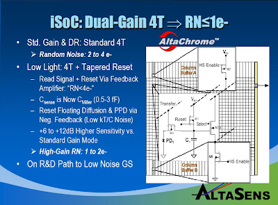
Altasens presents its new idea on tapered reset usage in 4T pixel on Intertech-Pira Image Sensors 2008 Conference. The pixel has 2 modes of operation. At large signal it works like any other 4T pixel. In low light mode the pixel transistor works in common source mode where the photodiode charge is transferred to its Miller capacitance. This way pixel has a higher gain, so that the column circuitry noise is less important. The slide below shows the idea:

Sony 1.4um Picture on Intertch-Pira Conference

Sony presented a picture from its new 8MP 1.4um pixel sensor on Intertech-Pira Image Sensors 2008 Conference. The picture is given below, as appeared in Sony .pdf file. Essentially, this is a copy of the picture from the official Sony PR, but with higher resolution and illumination conditions reported. The picture is quite good for a first generation sensor (click on it to expand):