While we are at HDR issues, TI proposes an improved way to mix two differently exposed images in its application US20090002530. To cope with mismatches and noise, TI employs linear regression and adaptive filter for noise gap reduction between high-gain and low-gain outputs of an HDR sensor.
Application US20090001257 from unknown Korean company (looks like Samsung to me) proposes to align the microlens with the active area, rather than the top metal. Normally in the process each subsequent layer is aligned with the previous one, so as third metal is aligned to second metal, which is aligned to the first one, which is aligned to poly or active. So, the misalignment is accumulated over many layers, increasing optical path variations. Being able to align microlens to active is an obvious idea, but to the best of my knowledge, this is impossible with any meaningful accuracy. Unfortunately, the application does not describe how exactly the stepper should be modified to achieve this alignment. I'm unable to find what company filed this application, but if somebody is able to align microlens straight with active layer, it would be a tangible advantage.
Dongbu application US20090004770 looks like a process engineer report on 400-450C final annealing influence on dark current non-uniformity and metal sheet resistance - a lot of low-temp annealing comparison data with some analysis. The experimental data is based on what looks like Foveon X3 sensor with 3.3um pixels made in 0.18um 1-poly 5-metal process. I'm not sure it's worth a patent, but it's certainly an interesting read for those who learn to deal with pixel optimizations.
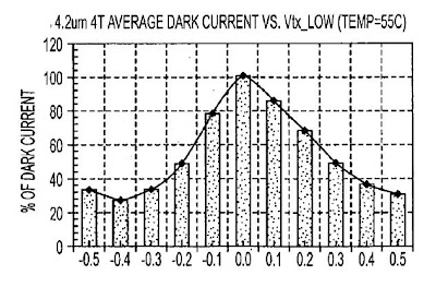
Micron's application US20080266435 talks about the ways of dark current reduction by biasing 4T pixel transfer. The claim is that with proper transfer gate engineering both positive and negative bias improve dark current and hot pixel rate. With positive bias depletion region under transfer gate creates a path for thermally generated to the floating diffusion. The negative bias increases the thermal electrons recombination rate. All these claims are supported by the nice graphs for different pixel sizes, such as one below:

The positive gate bias has an advantage of better blooming suppression, while the negative bias does not cause full well degradation.
I doubt that this patent would be granted in its broad form. Many companies for years use negative transfer gate bias exactly for the purpose of dark current reduction. Some use positive bias for different purposes too. But the application has an extension - a circuit which changes the bias depending on light conditions - this portion has chances to become a patent.
micron explained negative voltage reduction of DC by "recombination of DC electron with holes" --> if this is the mechnisim I would expect strong non-linearty at low illumination.
ReplyDeletemy alternative explantion is that in negative voltage the interface between TG GOX and TG Channel is pinned --> thus elimnating contributuion of DC from surface traps.
A.L
If one looks on the Micron's timing diagrams, the negative voltage is applied for the most part of the acquisition time, but not all. The transfer gate goes to zero some time before the readout starts, so that the linearity impact is minimized.
ReplyDelete