IEEE Spectrum published a podcast talking about tiny Awaiba camera for endoscopy (no video, just audio podcast):
Thursday, April 28, 2011
Yole Developpement Wafer Bonding Review
Yole Developpement published "Permanent Wafer Bonders: Technologies, Applications & Markets Report". The report sampler summarizes the approaches for BSI processing:


Wednesday, April 27, 2011
Vertical Transfer Gates Proposed by Omnivision, KETRI
Aiming to improve fill factor in small pixels, both KETRI and Omnivision applied for patents on vertical transfer gate structures, US20110084322 and US20110089311 respectively. The structures look quite similar:
Meanwhile, applications from Apple Imaging Group continue to trickle in. A large 91-page US20110090351 talks about temporal noise filtering with motion artifact reduction. The algorithm itself is quite straightforward but assumes that one has pixels motion vectors ready:

The Apple application also talks about other ISP stages, such as shading correction, defect pixel correction, demosaicing, etc.
 |
| KETRI Gate |
 |
| Omnivision's Gate |
Meanwhile, applications from Apple Imaging Group continue to trickle in. A large 91-page US20110090351 talks about temporal noise filtering with motion artifact reduction. The algorithm itself is quite straightforward but assumes that one has pixels motion vectors ready:

The Apple application also talks about other ISP stages, such as shading correction, defect pixel correction, demosaicing, etc.
Thursday, April 21, 2011
Aptina Announces 3.1MP 1080p/60fps HDR Sensor
Business Wire: Aptina announces AR0331 sensor aimed at security and surveillance applications. The 1/3-inch 3.1MP sensor features the new 2.2um pixel based on Aptina A-Pix tech and 100dB WDR capability with built-in adaptive local tone mapping. The new sensor provides HD video of up to 1080p at 60 fps employing binning techniques to enable the sensor’s sub 1-lux low light performance.
Sampling now, Aptina’s AR0331 mass production is scheduled for Q4 2011.
Sampling now, Aptina’s AR0331 mass production is scheduled for Q4 2011.
TYZX Demos Consumer Gesture Control
TYZX published Youtube video demoing its gesture control used by Samsung and Reactrix:
TYZX also opened Youtube channel showing its capabilities.
TYZX also opened Youtube channel showing its capabilities.
Tuesday, April 19, 2011
PTC and FD Capacitance Nonlinearity
The latest post in Albert Theuwissen's PTC series discusses pixel non-linearity and its effects on PTC.
Monday, April 18, 2011
EDoF vs AF Comparison
All About Symbian publishes a nice comparison of EDoF and AF camera phones. Nokia E52, E55, E5, E6, E7, C6-01, C7, and X7 phones are EDoF-based, while E72, X6, and N8 have AF cameras.
Friday, April 15, 2011
Canon Applies for Patent on Two-Row Parallel Output Pixel Layout
I do not believe this patent will ever be granted. Canon US20110080492 application talks about pixel layout allowing two rows to be read out simultaneously through two parallel column output lines. The idea to speed out pixel array with parallel outputs is now new, so it looks like Canon is trying to patent a specific layout implementation of it. Few layout versions are given, here is one of them:

Thursday, April 14, 2011
Altasens Raises $15.1M
TMCnet: AltaSens has raised $15.1M out of planned $20.1M in private equity offering. Investors are not disclosed.
Update: Here is Altasens SEC filing.
Update: Here is Altasens SEC filing.
NIT Announces 720p Color WDR Sensor
New Imaging Technologies announced release of its NSC1005 HD Ready sensor operating in 720p mode.
The NSC1005 has 1280x720 pixels of 5.6um size, with microlenses and/or color bayer filters. NSC1005 operates in rolling shutter mode up to a frame rate of 60fps. NIT's Native WDR technology is said to provide an instantaneous DR of more than 140dB, a logarithmic response of the signal. A custom de-bayerisation algorithm is available upon request from NIT in order to operate in the logarithmic response domain.
The NSC1005 has 1280x720 pixels of 5.6um size, with microlenses and/or color bayer filters. NSC1005 operates in rolling shutter mode up to a frame rate of 60fps. NIT's Native WDR technology is said to provide an instantaneous DR of more than 140dB, a logarithmic response of the signal. A custom de-bayerisation algorithm is available upon request from NIT in order to operate in the logarithmic response domain.
Omnivision Announces 1.4um 12MP BSI Sensor with EIS
PR Newswire: Omnivision launches a 12.6MP RAW image sensor supporting 1080p/60fps video with electronic image stabilization (EIS) aimed at high-end feature phones and smart phones.
The new OV12825 is built on OmniVision's proven 1.4-micron OmniBSI pixel architecture with sensitivity of 650 mV/(lux-sec). The sensor's binning capability further increases sensitivity in 1080p HD video mode at 60 FPS, while still providing additional pixels for EIS.
The OV12825 has an active array of 4,224 x 3,000 OmniBSI pixels operating at 15fps at full resolution. Its interfaces include 4-lane MIPI, LVDS and DVP. The sensor is currently available for sampling, and volume production is expected to begin by the second quarter of 2011.
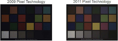
While we are at Omnivision, here are few slides from its March 2011 investors presentation:


OmniBSI low-light progress, 10 lux light at 8M 1/15s exposure (click to enlarge):
The new OV12825 is built on OmniVision's proven 1.4-micron OmniBSI pixel architecture with sensitivity of 650 mV/(lux-sec). The sensor's binning capability further increases sensitivity in 1080p HD video mode at 60 FPS, while still providing additional pixels for EIS.
The OV12825 has an active array of 4,224 x 3,000 OmniBSI pixels operating at 15fps at full resolution. Its interfaces include 4-lane MIPI, LVDS and DVP. The sensor is currently available for sampling, and volume production is expected to begin by the second quarter of 2011.
While we are at Omnivision, here are few slides from its March 2011 investors presentation:


OmniBSI low-light progress, 10 lux light at 8M 1/15s exposure (click to enlarge):

Wednesday, April 13, 2011
EETimes Interviews David Orton, Aptina CEO
EETimes published a big 3-page article based on interview with David Orton, CEO of Aptina. Some interesting points in no particular order:
- Aptina will no longer develop its own proprietary process technology beyond the 90-nm node. The company will begin working with outside foundries at 65-nm and beyond. Orton did not say which foundries Aptina will work with in the future, although some believe TowerJazz Inc. could be the first one.
- Since Micron entered the CMOS image sensor business, its image sensor products have been made in Micron’s 200-mm fab in Avezzano, Italy. More recently, some of the production comes from a Micron fab in Nishiwaki City, Japan. TowerJazz recently proposed to buy the Micron's Nishiwaki City fab for $140 million.
- Aptina will still need to embrace a foundry that has 300-mm capacity and can process wafers at 65-nm and below.
- Aptina’s rivals, namely OmniVision and Samsung, are currently growing faster in the marketplace, according to Robert Lineback, an analyst with IC Insights. "Aptina has been stuck with Micron's older 200-mm memory fabs as a primary foundry source, and that has hampered their efforts at the leading edge," Lineback said.
- In 2010, Aptina was ranked third in worldwide CMOS sensor sales, with $619 million in revenue, up 15 percent over 2009, according to IC Insights. Aptina was behind No. 2 Samsung ($624 million in 2010 sales, +24 percent from 2009) and No. 1 OmniVision ($795 million, +51 percent), according to IC Insights. STMicroelectronics was No. 4 ($569 million, +36 percent), and Sony was No. 5 ($548 million, +27 percent from 2009, according to the firm.
- "Overall, the CMOS image sensor business grew 17 percent in the 2010 recovery year to $4.5 billion from nearly $3.9 billion in 2009, when revenues dropped 16 percent in the downturn," Lineback said. "Compared to the entire optoelectronics market and semiconductor industry, CMOS image sensors had a relatively weak recovery due to pricing pressures in camera phones and some inventory adjustments in late 2010." CCD image sensors registered an increase of 25% to $3.3 billion in 2010 from $2.6 billion in 2009 while overall IC sales grew 32% in 2010 to $314.2 billion, according to IC Insights. "We now see CMOS image sensor sales growing by 13 percent in 2011 to a new record-high of $5.1 billion, which will exceed the previous peak of $4.6 billion set in 2008," Lineback said.
- Aptina continues to accelerate its efforts in the 1.4- and 1.1-micron (and beyond) pixel-size race after falling behind the competition.
- In 2006, some 90% of Aptina sales were in the mobile front, where its customers included Motorola and others. Today, some two-thirds of the company’s sales revolve around non-mobile applications, such as automotive, digital still cameras, industrial/military and surveillance.
- Aptina's sensors are incorporated in Nintendo's new 3DS handheld.
- Aptina must play catch-up in the smartphone/tablet market. "We fell behind in key technology," Orton said.
- Aptina’s "90-nm process got delayed," Orton said. "It took us longer than we thought." The company began shipping CMOS sensors based on the 90-nm process in the second half of last year. But this in turn delayed its 1.4um sensors-a move that "hurt" its bottom line.
- Aptina's recently announced 1.1um BSI pixels are based on a 90-nm process.
- Aptina's first BSI product, the 1/3.2-inch 1.4-micron 8-MP AR0833 is expected to sample starting in mid-2011.
- In the second half of 2011, Aptina expects to sample 1.1-micron BSI products including a 12-MP 1/3.2-inch and an 8-MP 1/4-inch sensors.
Tuesday, April 12, 2011
CMOSIS Announces its First Granted Patent
CMOSIS announces that on Feb. 1, 2011 the USPTO published its granted patent No. 7,880,662. This patent covers CMOSIS column parallel ADC as implemented in the the off-the-shelf image sensors CMV2000 and CMV4000 and several custom image sensor developments.
The patented ADC is of the counting ramp type combined with CDS in the digital domain and said to result in very low FPN. The prior art ADC with digital CDS has up and down counter to subtract the reset level from the signal level:

CMOSIS patented solution only needs a counting in one direction, while the subtraction is achieved by changing the timing logic. There are two version of counting logic presented:


Another advantage of the proposed ADC logic is that the full conversion can be achieved with just one analog ramp. In that case the comparator offset can be controllably changed between the signal and reset samples and the same counter can be used:

There are more techniques described in the patent, such as its application for TDI, pulse stretching or shrinking and clock interpolation.
iSuppli on Japan Image Sensor Industry Hit by Disaster
iSuppli's analyst Pamela Tufegdzic released a report "Japan Disaster Hits CMOS Image Sensors". Few quotes from the report:
"Toshiba Corp.’s Iwate Image Sensor fab, which produces logic chips and CMOS image sensors for mobile phone cameras, was shut down. Likewise, delivery was delayed from Sony Corp.’s CMOS image sensors to cell phone original equipment manufacturers.
Toshiba in 2010 was the world’s fifth-largest supplier of handset image sensors with 13.1 percent share of global revenue, according to a preliminary IHS iSuppli estimate. Sony ranked sixth with 3.9 percent share. Together, the companies accounted last year for 17 percent of the global handset digital camera image sensor revenue.
CCDs appear to be unaffected, at least for the near term. Altek Corp. and Ability Enterprise, which contract-manufacture products for major Japanese brand names, said they were not experiencing any shortages in near-term CCD supply from Japan. Ability now sources about 90 percent of its CCD components from Sony, while Altek buys between 70 and 80 percent of those parts from Sharp. Sharp’s CCD plants in Japan are far from the worst-hit zones, while Sony’s CCD plants are located in Thailand."
Update: EETimes adds that Toshiba's Iwate fab was due to resume partial operation in April, but the plant was hit by the strong aftershocks of April 7 and April 11. That plant is now due to restart partial production on April 18.
Monday, April 11, 2011
Chipworks: Fujifilm F550EXR BSI Sensor Made by Toshiba
Chipworks reverse engineering report revealed that Fujifilm's F550EXR BSI sensor with unusual color filter pattern and 1.4um pixel size is made by Toshiba, part number TCM5103PL. Here is the famous EXR pattern from Fujifilm site:
Update: 3 years ago Fujifilm decided to transfer its CCD front-end production to Toshiba. Now it seems that the agreement has been extended to CMOS sensors as well.
 |
|
Update: 3 years ago Fujifilm decided to transfer its CCD front-end production to Toshiba. Now it seems that the agreement has been extended to CMOS sensors as well.
Chipworks: Sony Switches to Bulk BSI in 1.1um Pixel
Chipworks is preparing the analysis of Sony’s latest 1.1um pixel sensor, the IMX081. Built on a 90 nm process, Sony has implemented a new pixel layout and schematic architecture, moving to an eight-shared pixel architecture (1.375T per pixel effective). One of the most interesting findings is that Sony has migrated to using bulk silicon substrates instead of SOI.
Here is the image (the smoking gun) that proves that Sony has indeed adopted a bulk Si process:

Here is the image (the smoking gun) that proves that Sony has indeed adopted a bulk Si process:

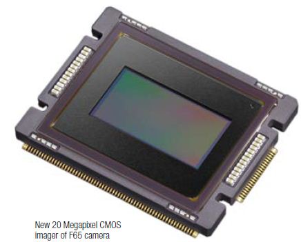
Sony ClearVid Lands in Digital Cinema Cameras
Film and Digital Times: Sony new 8K digital cinema cameras are going to use diagonal Bayer pixel arrangement, formerly known as ClearVid in consumer camcorders. The newly announced Super35-format F65 camera is reported to have that 45% angled CFA:

The new F65 sensor is reported to have 20MP resolution and send 16-bit raw data at speed of 20Gbps. The optical array area is 24.7 x 13.1 mm, diagonal is 28 mm.

The sensor is manufactured at Sony Kumamoto Technology Center, 300mm wafer line. The processing time is reported to be "up to 90 days".

Another Sony-Pro announcement is a stereo 3-CMOS sensors shoulder camcorder PMW-TD300. 6 half-inch sensors per camcorder - this market is starting to look more interesting!
Update: DCinema Today published the Sony's F65 sensor PR saying that the 20MP sensor can run at 120fps speed.

The new F65 sensor is reported to have 20MP resolution and send 16-bit raw data at speed of 20Gbps. The optical array area is 24.7 x 13.1 mm, diagonal is 28 mm.
The sensor is manufactured at Sony Kumamoto Technology Center, 300mm wafer line. The processing time is reported to be "up to 90 days".

Another Sony-Pro announcement is a stereo 3-CMOS sensors shoulder camcorder PMW-TD300. 6 half-inch sensors per camcorder - this market is starting to look more interesting!
Update: DCinema Today published the Sony's F65 sensor PR saying that the 20MP sensor can run at 120fps speed.
Sunday, April 10, 2011
Samsung Applies for Combined ToF and RGB Imager Patent
Samsung application US20110074989 proposes the integration of ToF IR pixels with RGB or RGB-W ones in a single array. One example of the pixel arrangement assumes quite big structure repeating itself across the array (black area transmits IR light):

The cross-section along the lines A-A is:

ToF portion seems to be based on Kawahito ToF approach with in-phase and out-of-phase integration nodes, controlled by electric current flow, Fig 5A and B respectively:

At the same time RGB-W pixels are protected from IR ToF illumination by a p+ potential barrier:

The sensor seems to be aimed to mobile applications.
Update: A separate Samsung application US20110085063 talks about IR-RGB color filter arrangement and RGB interpolation for that case.
Friday, April 08, 2011
Photodiode Advances Reviewed
Croatian open-access publishing house InTech published a book titled "Advances in Photodiodes", available for free download. The book is a collection of papers on various aspects of photodiodes, Si-based and other materials. Some of the interesting chapters include:
Spectral Properties of Semiconductor Photodiodes
Terubumi Saito
Noise in Electronic and Photonic Devices
K. K. Ghosh
Performance Improvement of CMOS APS Pixels using Photodiode Peripheral Utilization Method
Suat U. Ay
Avalanche Photodiodes in Submicron CMOS Technologies for High-Sensitivity Imaging
Gian-Franco Dalla Betta, Lucio Pancheri, David Stoppa, Robert Henderson and Justin Richardson
Thanks to JR for sending me the link!
Thursday, April 07, 2011
1B Camera Phones to be Sold in 2011
Beta News got a hold of Strategy Analytics report on global camera phone sales. The report forecasts that camera phones will exceed one billion per year for the first time in 2011. This represents a 21% growth over the 918 million sold worldwide in 2010, and solidifies the mobile phone image sensor as the most successful mobile peripheral ever developed.
"The fastest growing segment of the camera phone market will be the high-tier," Neil Mawston, Director at Strategy Analytics said on Thursday. "We forecast camera phones with sensors of eight megapixels and above to grow a healthy 240 percent worldwide during 2011."
"The fastest growing segment of the camera phone market will be the high-tier," Neil Mawston, Director at Strategy Analytics said on Thursday. "We forecast camera phones with sensors of eight megapixels and above to grow a healthy 240 percent worldwide during 2011."
1.3MP Reported to be in Tight Supply in China
Digitimes: The 1.3M sensors have been in tight supply in China since November 2010 as most tablet PCs, mainstream handsets and digital toys rolled by local makers include a 1.3MP sensor, Digitimes' sources said. The tight supply is expected to ease in the second half as OmniVision will begin to ramp up its output of 2MP imagers in May, indicated the sources. OmniVision is currently accounting for an over 30% share in China.
New CFA, Rectangular Pixels Proposed
A Seattle based startup Image Algorithmics proposes a new, better CFA combined with rectangular pixels. Regular Bayer CFA relies on 3 colors and square pixels:

The proposed CFA best works with rectangular pixels with aspect ratio 1.41:1 and has 4 colors, each of them is a linear combination of red, green and blue:

Although the physical pixels are rectangular, the color image processing seems to convert them in usual square-shaped pixels.
In comparison with the Bayer CFA with the same pixel count, same resolution, same chrominance bandwidth and demosaicked with the popular AHD algorithm, the proposed pattern is claimed to have the following advantages:
The main principles of the proposed CFA-pixel-algorithm combination are discussed in SPIE IS&T Electronic Imaging 2011 paper here.

The proposed CFA best works with rectangular pixels with aspect ratio 1.41:1 and has 4 colors, each of them is a linear combination of red, green and blue:

Although the physical pixels are rectangular, the color image processing seems to convert them in usual square-shaped pixels.
In comparison with the Bayer CFA with the same pixel count, same resolution, same chrominance bandwidth and demosaicked with the popular AHD algorithm, the proposed pattern is claimed to have the following advantages:
- 7.6dB PSNR improvement on the Kodak image set
- Even greater, 10dB PSNR, improvement on realistic images
- Greatly reduced artifacts
- One quarter as much increase in MSE due to noise. This is because of:
a. lighter filter colors that let in more light
b. no directional sensing algorithms to get confused by noise
c. numerically stable demosaicing, unlike CMY patterns - Uniform quantum efficiency - hence resistant to sensor saturation
- Low complexity demosaicing using separable filters, can be used in phone camera video
- Simple noise characterization resulting in more effective post demosaicking noise reduction
- Chromatic Aberration correction can be performed after demosaicing with an order of magnitude less increase in MSE than Bayer
The main principles of the proposed CFA-pixel-algorithm combination are discussed in SPIE IS&T Electronic Imaging 2011 paper here.
Tessera Explores Separation of Imaging & Optics Business
Tessera announced that it is exploring a possible separation of Imaging & Optics business. The company is evaluating multiple alternatives, including spin-off.
Tessera has not set a timetable for completing its exploration and there can be no assurance that the process will result in any transaction. The company does not expect to make further public comment regarding these matters unless a definitive agreement or other commitment for any transaction is reached.
Tessera has not set a timetable for completing its exploration and there can be no assurance that the process will result in any transaction. The company does not expect to make further public comment regarding these matters unless a definitive agreement or other commitment for any transaction is reached.
Wednesday, April 06, 2011
Teledyne and Raytheon Receive 2011 Herschel Award
PR Newswire: Raytheon Vision Systems (RVS) and Teledyne Imaging Sensors receive 2011 Herschel Award for the development of state-of-the-art hybrid visible FPA solutions based on Silicon P-i-N detector technology. These FPAs have superior performance in quantum efficiency, radiation hardness and spectral response relative to other more conventional imaging arrays. The award was presented at the 2011 Military Sensing Symposia held in Orlando, FL.
ST Proposes Red-Reflective BSI Pixel
ST patent application US20110073976 aims to solve red QE problem by making a reflective STI pattern 41 as shown on the figure:
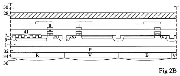
A prior art achieving reflection from metals on the front side was rejected due to "in microelectronics, all metals are normally processed and deposited to be non-reflective. Introducing a reflective metal layer may require significant modifications of the manufacturing conditions," and "insertion of an additional metal element in the structure has the disadvantage of causing stray capacitive couplings."
"Unevennesses 41 form a periodic pattern formed of pads surrounded with trenches. These pads may have a square base, but will preferably have a circular or hexagonal basis to avoid privileging a specific type of light biasing. Period Λ of the pattern, height d of the pads, as well as the ratio between the width of the pads and the width of the interval separating them are selected so that the periodic unevennesses altogether form a two-dimensional optic network capable of reflecting wavelengths corresponding to the color red of the visible spectrum."
"For a photodiode associated with a red filter, unevennesses 51 [typo, meant to be 41 - ISW] will, for example, have the following characteristics: period Λ: on the order of from 350 to 400 nm; height d of the pads: on the order of from 50 to 300 nm; ratio between the pad width and the distance between pads close to 1."
"An advantage of such a structure is that the reflection effect is better with a two-dimensional network than with a reflective layer. Another advantage is that this result is obtained without introducing any new material with respect to known structures."
Adimec Machine Vision Blog
Adimec blog on machine vision topics occasionally has image sensor articles, like CCD to CMOS comparison for machine vision cameras. One can see that vision applications are still using relatively large proportion of CCDs:

Tuesday, April 05, 2011
IISW 2011 Announcement
The Co-Chairmen of the 2011 IISW have determined that the workshop will continue in Hokkaido Japan as planned. All indicators at the conference site are 100% normal. Participants can fly to Hokkaido via South Korea or western Japan.
Cancellation policies are being adjusted and participants will receive email from the conference organizers in Japan soon discussing this and other details. Presenters that are unable to come to Hokkaido in person will be allowed to submit their paper and possibly present their work by voice or video. Based on a survey of participants, we expect about 20-25% of the original participants to be impacted. Samsung Electronics graciously made back up arrangements in South Korea for the 2011 IISW but the survey found that this only reduced the participation impact by about 50%. While the situation for the 2011 IISW is not ideal, we hope the community will forgive any inconvenience and recognize that it pales in comparison to the situation faced by hundreds of thousands of Japanese people.
Sincerely,
Eric R. Fossum
President, ImageSensors Inc.
A California Non-Profit Public-Benefit Corporation
for the 2011 IISW Organizing Committee
Eedoo to Compete with Xbox on Gesture Recognition
Reuters: I missed this news from about half a year ago that China-based company Eedoo plans to release its own eBox equipped with camera with gesture recognition. The company has been spun-off from Lenovo. eBox is to be sold in China only.
Eedoo claims to be the No. one in China and No. two in the world with full body gesture recognition in game console. Talking about the gesture-recognition camera portion, China Daily newspaper published a figure on how it works:

The published console images from Kotaku site show a camera on top of TV that looks very similar to many other 3D depth-sensing ones:

Eedoo claims to be the No. one in China and No. two in the world with full body gesture recognition in game console. Talking about the gesture-recognition camera portion, China Daily newspaper published a figure on how it works:
The published console images from Kotaku site show a camera on top of TV that looks very similar to many other 3D depth-sensing ones:
Altera, Apical, AltaSens Jointly Develop WDR Chipset
PR Newswire: The WDR chipset combines an Altera Cyclone IV E FPGA with a security chip that supports Apical's HD WDR full ISP pipeline IP and AltaSens' 1080p60 A3372E3-4T image sensor. Apical's HD HDR full image signal pipeline IP is optimized to take advantage of the capabilities of the Altera FPGA. No other application ASSP or DSP platform is said to offer WDR technology using a 1080p60 sensor and a comprehensive datapath (a full HD raster is 2200x1125 pixels x 16+ bits per pixel x 60 frames per second, resulting in >2 Gbps bandwidth). The solution offers:

- Hot pixel removal and noise reduction (spatial and temporal IP cores are available)
- Advanced per pixel tone mapping (Apical's patented Iridix IP core)
- Advanced demosaic and color correction
Monday, April 04, 2011
TowerJazz Buys Micron's Fab in Japan
I haven't seen the official PR yet, but Reuters, Globes, EETimes, and many other sources report that TowerJazz is to acquire Micron's fab in in Nishiwaki City, Japan for $140M in cash and stock transaction ($40M cash plus common stock plus some liabilities). The Micron facility is said to help TowerJazz target Japanese camera companies.
"We will be able to acquire some very good camera companies as end users," Russell Ellwanger, TowerJazz CEO, told Reuters. "We haven't been able to make progress with high-end camera users and having a presence in Japan opens up that opportunity for us." So far Japan only accounts for half a percent of TowerJazz' output.
The proposed purchase of the plant, located 600 km south of Tokyo, would increase TowerJazz production by 80 percent, or 60,000 wafers per month. The facility is said to have not been affected by the earthquake and tsunami in Japan last month.
Update: The official PR at Business Wire says that the Micron's facility can support geometries down to 95nm.
Anteryon Wafer Level Optics Presentation
Anteryon presented its wafer level optics solutions at Fotonica Evenement 2011 on March 30. The slides from "WaferOptics Mass Volume Production & Reliability" presentation speak for themselves:
Update: Anteryon asked me to remove the slides for two reasons:
Anterion may opt to send me other slides which the company feels more comfortable to publish.
Update: Anteryon asked me to remove the slides for two reasons:
- The slides contain some internal information that the company prefers not to see in public access
- The subset of slides I've happened to chose from the presentation seems to misrepresent the company's work.
Anterion may opt to send me other slides which the company feels more comfortable to publish.
PTC and QE Tutorial
Albert Theuwissen continues his series of PTC tutorials, now talking about QE, PRNU, FPN and their influence on QE measurements.
Lattice Announced HiSPi to Parallel Bridge
Market Wire: Lattice announced Aptina's High-Speed Serial Pixel Interface (HiSPi) to parallel bridge using LatticeXP2 FPGAs. The bridge allows any ISP with a traditional CMOS parallel bus to interface with an Aptina HiSPi CMOS sensor. This HiSPi bridge solution is aimed to security cameras, automotive applications, high end consumer cameras and other camera applications where the use of higher resolution and higher frame rate CMOS sensors is desirable.
Sunday, April 03, 2011
Saturday, April 02, 2011
April Fools' Gmail Motion
Google April Fools' Gmail Motion announcement was quite nice. While not directly image sensor related, it parodies fashionable gesture recognition projects:

Hynix Update: 1.4um, 1.1um Pixel Sampling
March Hynix Newsletter reveals recent Hynix advances in small pixel design: 2.0um and 1.75um pixels are in mass production now, 1.4um is at customer samples stage, 1.1um is to reach engineering sampling phase in April:


The full sensor line-up is shown in the new Q2 2011 Hynix catalog. Hynix says it aims to capture 20% of CIS market by leveraging its manufacturing strength in memory and a customer support system for the China market.
The full sensor line-up is shown in the new Q2 2011 Hynix catalog. Hynix says it aims to capture 20% of CIS market by leveraging its manufacturing strength in memory and a customer support system for the China market.
Friday, April 01, 2011
Omnivision Acquires 850 Kodak Patents for $65M
PR Newswire: OmniVision announced the purchase of approximately 850 image sensor-related patents and patent applications from Eastman Kodak for $65.0 million in a cash transaction. The transaction was completed on March 31, 2011.
"We are pleased with the opportunity to double the size of our intellectual property portfolio for CMOS image sensors," said Shaw Hong, CEO of OmniVision.
The purchased patent portfolio comprises approximately 850 U.S. and foreign patents and patent applications. The intellectual property includes numerous granted patents of key CMOS technologies covering early and fundamental CMOS image sensor work; improvements on foundational architectures, including new features and functions; and next generation performance improvements, miniaturization and cost reduction technologies.
Sue-Me Announces BIS Sensor
Adorama News: A dramatic advance in image sensor technology has been announced by Sue-Me corporation. The company's new sensors feature Backside Irrigated Sensors (BS) with backside liquid cooling, which they claim can take perfectly clear, detailed and accurate photos in complete darkness, with an ISO range from 100 to 1,000,000,080. A low-light test photo captured by BS Sensor pre-production camera:


Subscribe to:
Posts (Atom)